The global market for Fpga Integrated Circuit technology is expanding beyond traditional telecommunications and industrial control. Grand View Research estimated the FPGA market at approximately USD 9.5 billion in 2022, with strong growth expected through 2030. MarketsandMarkets projects a different trajectory, forecasting growth from about USD 12.1 billion in 2023 to USD 19.2 billion by 2028. These figures are not identical. Market definitions vary, and that deserves careful attention.
Demand is rising in artificial intelligence, automotive radar, aerospace systems, medical imaging, and edge computing. A modern FPGA can process parallel workloads while preserving field-level reprogrammability. That balance matters when product requirements change quickly. It also affects power budgets, thermal design, and long-term maintenance. Near a production line, for example, an engineer may update logic without replacing the entire control board.
Steve Trimberger, a prominent FPGA architect and former Xilinx Fellow, described FPGAs as “the Swiss Army knife of computing.” The comparison is practical, not perfect. Flexibility can increase design complexity, verification time, and development cost. Leading manufacturers therefore compete through architecture, software ecosystems, chiplet integration, security features, and manufacturing capacity. Companies such as AMD, Intel, Lattice Semiconductor, Microchip Technology, and Achronix serve different performance and power segments.
This guide examines the top FPGA Integrated Circuit manufacturers worldwide. It considers product families, process technologies, application strengths, developer tools, and market positioning. Financial rankings alone can mislead. A smaller supplier may offer better efficiency for a specific embedded design. Real engineering results depend on workload, tool quality, supply continuity, and technical support. Expect variation. That is the point.
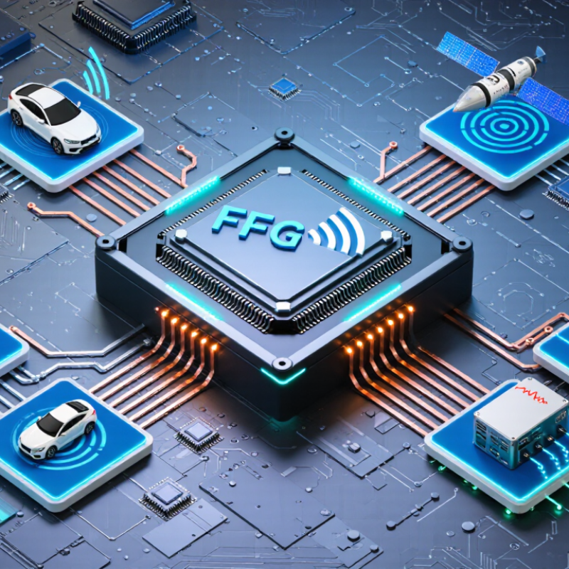
An FPGA integrated circuit is a reprogrammable semiconductor device. It performs digital operations without requiring a new silicon design for every change. Unlike a fixed-function chip, an FPGA can be configured after manufacturing. Engineers load a hardware description, then test the resulting logic on physical equipment. This flexibility shortens development cycles. It also introduces design complexity.
Inside an FPGA, configurable logic blocks process Boolean operations and arithmetic tasks. Look-up tables, or LUTs, define these logic functions. Flip-flops store results between clock cycles. Programmable routing connects separate logic regions across the chip. Many devices also include embedded memory, clock-management circuits, digital signal-processing blocks, and high-speed transceivers. The architecture resembles a city with adjustable roads. Congestion can still reduce performance.
Core functions include data filtering, protocol conversion, parallel computation, and real-time control. A designer might process sensor samples while another logic region manages a communication interface. Parallel hardware can complete several operations within one clock period. However, faster clock speed alone does not guarantee better results. Timing paths, power limits, and memory access often decide actual performance.
Worldwide FPGA manufacturers usually offer devices for industrial, communications, automotive, scientific, and aerospace applications. Reliable selection requires checking operating temperature, package quality, configuration security, and long-term supply support. Laboratory testing should include voltage variation, thermal cycling, and fault recovery. I would not treat a data sheet as final proof. Board layout, firmware quality, and verification discipline can expose weaknesses that the silicon specification never shows.

Top FPGA Integrated Circuit Manufacturers Worldwide
Leading FPGA manufacturers typically organize their products into several clear families. High-end families combine large logic capacities with fast serial transceivers, making them suitable for networking, imaging, and data-center acceleration. Mid-range families balance logic resources, memory, and power consumption for industrial control and test equipment. Low-power families target portable instruments, cameras, and embedded monitoring systems.
Product families often differ in more than gate count. Engineers compare lookup tables, embedded memory, digital signal blocks, package size, and thermal limits. Some families include integrated processors, allowing software and programmable logic to share one device. Others focus on simple reconfiguration and lower unit cost. During evaluation, a small development board can reveal timing issues that datasheets hide. It is a practical check.
Leading suppliers also offer radiation-tolerant, automotive-grade, and secure-device families. These versions usually include stronger qualification, wider temperature support, and protection against unauthorized configuration changes. However, product labels can be confusing. A device described as “low power” may still require careful clock planning and heat analysis. I have found that early power estimates are often optimistic. Designers should measure real workloads, not trust ideal benchmarks alone.
Tool support is another part of the product family. Mature families usually provide synthesis software, simulation models, reference designs, and long-term documentation. Smaller families may reduce cost but offer fewer interfaces or migration options. That trade-off matters. A reliable selection considers present performance, future availability, board layout, and the team’s debugging experience.
A manufacturer-neutral comparison of major FPGA product-family categories, typical capabilities, and common deployment areas.
| Product Family Category | Primary Architecture | Typical Process Technology | Typical Logic Capacity | Embedded Memory | DSP Resources | High-Speed Connectivity | Common Applications |
|---|---|---|---|---|---|---|---|
| High-End FPGA | Large LUT-based fabric with extensive programmable routing, hardened memory controllers, and dedicated arithmetic blocks | Approx. 7 nm to 16 nm | About 100,000 to more than 2 million logic elements | Distributed RAM, block RAM, and large embedded memory arrays | Hundreds to several thousand DSP-oriented blocks, depending on device size | Multi-gigabit serial transceivers, PCI Express, Ethernet, and high-bandwidth memory interfaces | Data-center acceleration, networking, telecom infrastructure, imaging, and high-performance computing |
| Mid-Range FPGA | Balanced programmable logic fabric with integrated RAM, DSP, clocking, and general-purpose I/O | Approx. 12 nm to 40 nm | About 20,000 to 500,000 logic elements | Block RAM and distributed memory suitable for buffering and control functions | Dozens to several hundred DSP blocks | PCI Express, Gigabit Ethernet, DDR memory, and selected serial transceivers | Industrial automation, machine vision, medical equipment, test systems, and embedded control |
| Low-Power FPGA | Compact LUT fabric optimized for low static and dynamic power consumption | Approx. 22 nm to 65 nm | About 2,000 to 100,000 logic elements | Small to medium embedded RAM capacity | Limited or moderate DSP resources | General-purpose I/O, low-voltage interfaces, and selected SERDES options | Portable electronics, consumer devices, battery-powered systems, and sensor hubs |
| FPGA with Integrated Processor System | Programmable logic combined with hardened application processors, memory controllers, and peripheral interfaces | Approx. 12 nm to 28 nm | About 50,000 to more than 1 million logic elements | On-chip RAM plus support for external DDR memory | Integrated DSP blocks for signal processing and hardware acceleration | Ethernet, PCI Express, USB, memory interfaces, and processor peripheral buses | Robotics, embedded Linux platforms, industrial vision, aerospace systems, and edge computing |
| FPGA Accelerator Family | Highly parallel programmable fabric designed for custom pipelines and workload-specific acceleration | Approx. 7 nm to 28 nm | About 100,000 to more than 2 million logic elements | Large block RAM, distributed RAM, and optional high-bandwidth memory support | High-density DSP resources for matrix, filtering, compression, and artificial-intelligence workloads | PCI Express, high-speed Ethernet, coherent host links, and multi-gigabit transceivers | Cloud computing, financial modeling, video processing, networking, and artificial intelligence inference |
| Radiation-Tolerant FPGA | Logic architecture designed for reliability under radiation exposure and harsh operating conditions | Approx. 65 nm to 180 nm, depending on qualification requirements | About 10,000 to 500,000 logic elements | Radiation-tolerant block memory and configuration-storage features | Application-dependent DSP and arithmetic resources | Space-qualified I/O, serial interfaces, LVDS, and mission-specific communication links | Satellites, launch vehicles, defense electronics, scientific instruments, and high-reliability control systems |
| Automotive-Grade FPGA | Programmable logic with functional-safety features, extended temperature support, and automotive interfaces | Approx. 16 nm to 65 nm | About 20,000 to 500,000 logic elements | Embedded RAM for sensor aggregation, buffering, and deterministic control | Moderate DSP capacity for radar, camera, and sensor-processing workloads | Automotive Ethernet, MIPI, LVDS, CAN-related system integration, and high-speed sensor links | Advanced driver-assistance systems, sensor fusion, in-vehicle networking, and display processing |
| Security-Focused FPGA | Programmable logic with secure boot, encrypted configuration, key management, and tamper-resistant features | Approx. 16 nm to 65 nm | About 20,000 to 1 million logic elements | Embedded memory with configuration-protection and access-control mechanisms | Dedicated or programmable resources for cryptographic and packet-processing workloads | Secure Ethernet, PCI Express, serial transceivers, and protected management interfaces | Critical infrastructure, defense, communications equipment, payment systems, and industrial security |
| Technical ranges are representative industry values rather than specifications for a single device. Actual capacity, process node, interfaces, memory size, and qualification level vary by manufacturer, device generation, package, and configuration. | |||||||
FPGA manufacturing begins with silicon process selection, architecture planning, and precise control of power and heat. Modern processes use smaller transistors to increase logic density and reduce signal delay. Yet smaller geometries can increase leakage, process variation, and thermal sensitivity. That trade-off matters. Manufacturers combine configurable logic blocks, routing networks, memory, and high-speed interface circuits on one die. They also use advanced packaging to improve bandwidth between the FPGA and external memory.
Design capability is measured beyond raw logic capacity. Experienced engineering teams study timing closure, clock distribution, signal integrity, and power behavior from the earliest design stage. In board bring-up, small routing decisions can create unexpected noise or timing failures. Practical verification therefore includes simulation, emulation, hardware testing, and long-duration workload checks. Strong development flows also provide reusable intellectual property, dependable design tools, and clear documentation. Tools are powerful, but they are not infallible.
Manufacturing reliability depends on wafer inspection, electrical probing, package testing, and screening across temperature ranges. High-performance devices may include hardened memory, digital signal processing blocks, security functions, and specialized transceivers. These features reduce design effort, although they can limit flexibility when requirements change. Packaging must manage heat through effective substrates, thermal paths, and carefully designed pin assignments. No design is perfect. A rushed power estimate can still undermine an otherwise capable device. Continuous measurement, independent review, and honest failure analysis remain essential when selecting FPGA manufacturing technologies.
FPGA manufacturing has progressed from mature 65/55 nm processes to advanced 7 nm technologies. The chart shows representative maximum high-speed serial transceiver rates publicly documented across FPGA technology generations. Newer process nodes generally support higher bandwidth, greater logic density, improved power efficiency, and more advanced programmable system integration. Actual performance varies by device architecture, package, protocol, and operating conditions.
FPGA integrated circuits support applications that need adaptable hardware and rapid data processing. A 2024 global FPGA market report estimates the sector could grow from about USD 9 billion in 2023 to nearly USD 14 billion by 2028. Data centers use FPGAs for network acceleration, encryption, and real-time analytics. They can process parallel workloads with lower latency than many general-purpose processors. However, power efficiency depends heavily on workload design and memory access.
Telecommunications equipment uses FPGAs to manage signal processing, beamforming, and evolving network standards. In industrial automation, engineers apply them to motion control, machine vision, and predictive maintenance systems. The International Federation of Robotics reported more than 500,000 industrial robot installations worldwide in 2023. Many of these systems need deterministic control. FPGAs can respond within strict timing windows, especially near cameras and sensors.
They also appear in medical imaging, aerospace systems, automotive radar, and scientific instruments. A 2024 automotive electronics study projects continued growth in advanced driver-assistance systems through the decade. FPGA-based prototypes help teams test algorithms before committing to fixed silicon. That flexibility saves redesign time, but it can increase verification effort. The difficult part is often not speed. It is proving long-term reliability under heat, vibration, and software updates. Market forecasts remain useful, yet their assumptions can change quickly with chip supply, energy costs, and regional regulations.
Comparing global FPGA manufacturers requires more than counting logic cells. Grand View Research estimates the FPGA market will expand at about 9% annually through 2030. That growth reflects demand from data centers, industrial automation, communications, and automotive electronics. Buyers should examine process technology, programmable logic density, embedded memory, DSP resources, and high-speed transceiver capacity. A larger device is not automatically better. Power efficiency matters when boards operate continuously in crowded racks.
Supply reliability is equally important. The Semiconductor Industry Association reported that global semiconductor sales reached approximately 627 billion dollars in 2024, showing strong but uneven demand across regions. For FPGA purchasers, manufacturing location, wafer access, packaging capacity, and average lead time deserve direct verification.
Lifecycle support also affects total cost. A device that remains available for ten years may outperform a cheaper part with uncertain continuity. Software quality should be tested through compilation time, debugging tools, IP availability, and field updates. These factors often decide engineering schedules.
Mordor Intelligence forecasts sustained FPGA market growth during the present decade, but market reports use different definitions and assumptions. Comparisons are imperfect. Regional pricing can change quickly with currency movements, export controls, and allocation pressure. Independent reliability records, documented thermal data, and sample-based testing provide stronger evidence than promotional specifications. Engineers should request production references and failure-rate data. Do not rely on headline performance alone.
Please share your email with us to see your results.